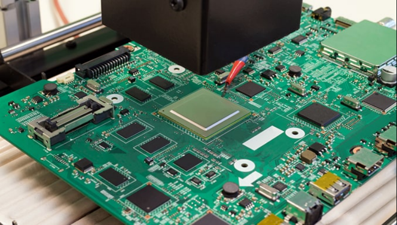
Many different problems can occur in PCB Assembly. These include missing components, displaced or twisted wires, using incorrect components, insufficient soldering, excessively thick joints, bent IC pins, and lack of wetting. To eliminate these defects, careful inspection of the assembled and soldered components is essential. However, components have become extremely small over the years, and 3D AOI is used to find complex defects.
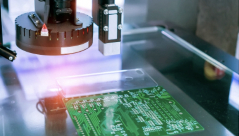
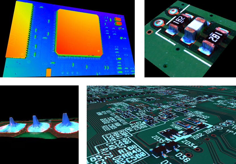
While 2D AOI relies on planar imaging to inspect components, using color contrast and grayscale analysis, 3D AOI utilizes advanced 3D imaging modules (e.g., single DLP projector + multi-angle cameras) to capture height maps and volumetric data. The obvious advantage is that 3D AOI can identify defects that are invisible to the naked eye (shadowed areas, e.g., under tall components like connectors or capacitors), reducing the number of defects that slip through the inspection process and can be more precise.
They are much more accurate because they take multiple images from different angles. A 3D AOI machine uses software to compare the PCB it inspects to the diagram it’s been programmed with. It then reports any discrepancies, including location, measurement of dimensions, and misalignment of components.
3D AOI is critical for advanced sectors:
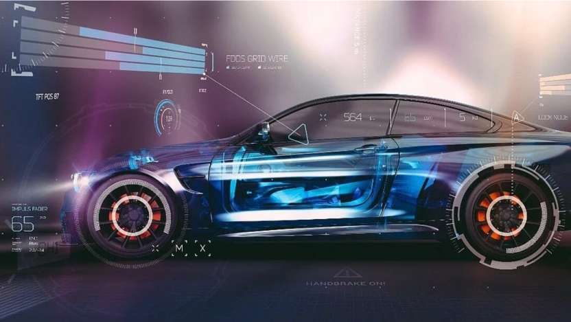
Automotive: Ensures reliability for safety-critical PCBs (e.g., ADAS modules)
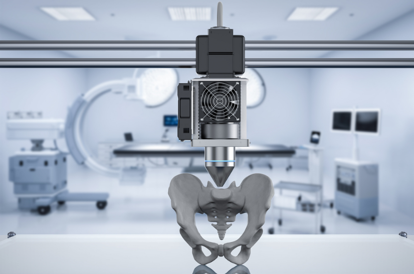
Medical devices: Validates solder integrity in implantable electronics.
Aerospace: Meets IPC Class 3 standards for high-reliability assemblies.
Some of their PCBAs are complex and have high density, which may pose hidden defect risks, such as smartphones, tablets, smartwatches, AR glasses, electronic control units, and advanced driver-assistance systems in vehicles, cardiac pacemakers, neurostimulators, portable monitors, industrial automation control modules, 5G base stations, optical communication equipment, etc. The PCBA in those industries that require micro-scale or high-density components shall use 3D AOI to detect BGA/LGA solder ball defects, such as micro-scale components like 01005 package components (0.4mm×0.2mm).

We have the capacity to produce these high-precision products for customers. And as a strategic investment in achieving manufacturing excellence, we use 3D AOI machines to improve the quality and efficiency of our PCB assemblies.
3D AOI’s value extends beyond defect detection to process optimization, cost control, and data-driven decision-making.
Process Optimization
1. Measures solder paste volume, height, and slump, providing real-time feedback to stencil printers (e.g., adjusting stencil pressure or squeegee speed) to prevent batch-level soldering defects.
2. Inspect various types of PCBs. It is a versatile tool for quality testing.
3. Supports multi-product detection (e.g., switching from TV motherboards to power adapter PCBs) with <5-minute switch time, aligning with high-mix, low-volume trends.
4. Detects mixed THT (through-hole) and SMT boards.
5. Looks at both sides of the board at once, faster and more efficient.
Cost Control
1. Detects soldering issues at the SMT stage (vs. post-assembly) lowers rework costs per board by 70% (no disassembly of enclosures/cables required).
2. Optimizes thermal profiling in reflow ovens, cutting energy waste by 15–25%.
3. Reduction in return rates for consumer electronics saves after-sales costs and avoids compliance risks.
Data-driven Decision-making
It can automatically identify spatiotemporal distributions of defect types (e.g., cold solder, misalignment) to pinpoint process issues (e.g., nozzle wear in pick-and-place machines, reflow oven anomalies).
Post time: Mar-31-2025